

These notes are for the early radios. It's not known if the wiring is the same in the late radios. Judging by the late schematics, it would seem it is the same.
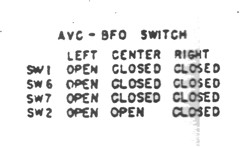
Wiring for the AVC BFO switch. Note orientation of wafer in the pictures below are the same. There are two contacts on the back side of the
wafer but since it is crimped to the switch frame, I was not able to photograph that side.
From the schematic.


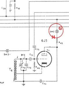

V7 Top Cap
Ground
No connection.
Goes to the junction of R61, C66 and SW8-15. On an early radio (s/n H_118969), there does not appear to be
an SW8-15. There are no contacts on the side of the wafer facing the oscillator module chassis. I do
not have a schematic that shows this.
V8 pin 8, R58, R59, C63, C64
No connection.
B+
Goes to R45 which goes to the plate of V11.
Goes to R11. R11 is located on T21 in the mixer section.
Page: /AVC_BFO_switch/AVC_BFO_switch.shtml
Last modified: Friday, 24 Apr 2026