
On my Pixel cell phone, I asked Gemini how to hook up a signal generator to the antenna inputs and got what is
presented here. For clarification, I repeated the prompt on a desktop PC logged into the same Google account and
got a much abbreaviated (and incorrect) answer1.
I repeated the exact prompt on the cell phone and got a completely diffirent answer.
It turns out that this is the way AI works and the reason why is interesting (I asked) but
it doesn't belong here.
The source2 is here.
This entire page is AI generated and reformatted to suit this website. The original schematic did not fit
on the output page so a scroll bar was included. I captured the left and right halves and made a complete image.
I had my doubts though. An "L-pad" has 2 resistors and a Pi or "T-pad" has 3. In the circuit below, the 211 Ω resistor
is supposed to be the result of 426 and a 419 Ω resistors in parallel - one from the L pad and one from the 1st Pi pad.
I asked Gemini another question (see below) and got a result that leads me to believe the "*" next to the 211 Ω resistor
was in error. Additional questions supported the 211 Ω value. Very confusing. By trying to make the result simpler, it became
more difficult to understand.
Created with 3 Flash June 28, 2026 at 03:40 AM Published June 28, 2026 at 03:42 AM
To transform a 1 mV p-p signal from a 50 Ω source down to a 1 µV p-p signal into a 400 Ω load, you need to accomplish two distinct goals:
Impedance Matching: Transform the 50 Ω source up to 400 Ω to maximize power transfer (or minimize reflections).
Voltage Attenuation: Safely drop the voltage down to the target 1 µV p-p while maintaining that 400 Ω environment.
Because a passive, lossless impedance match from 50 Ω to 400 Ω naturally increases voltage by a factor of
the matching network alone will bring your 1 mV signal up to about 2.83 mV. From there, you will need a massive 69 dB attenuation pad to drop it down to 1 µV.
Here is how to design the circuit using standard resistive networks, which work perfectly from DC up to high RF frequencies.
The most reliable approach is a two-stage network: an asymmetrical resistive matching pad (L-pad) to transition from 50 Ω to 400 Ω, followed by a 400 Ω Pi (π) or T-pad attenuator to handle the huge voltage drop.
To match a low impedance (R1 = 50 Ω) to a higher impedance (R2 = 400 Ω), we use a series resistor (Rs) and a shunt resistor (Rp).
Series Resistor (Rs):

Shunt Resistor (Rp, placed on the 50 Ω side):
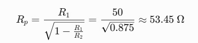
Stage 1 Performance:
Impedance looking left: 50 Ω
Impedance looking right: 400 Ω
Voltage Insertion Loss: This pad introduces a voltage loss. Looking from the 1 mV source, the voltage at the 400 Ω output of this matching pad drops to exactly 0.3536 mV p-p.
Now we need to step down from 353.6 µV (the output of Stage 1) to your target 1 µV.
Required Target Attenuation Ratio: 353.6/1 = 353.6
Required dB Attenuation: 20log10 (353.6) ≈ 51 dB
Because a single-stage 51 dB attenuator requires incredibly sensitive resistor values that are easily ruined by stray parasitics, it is best split into two cascaded 400 Ω Pi-pads (e.g., a 30 dB pad followed by a 21 dB pad).
For a standard 400 Ω Pi-pad, the resistor values are calculated as follows:
Pad A: 30 dB Attenuation (400 Ω environment)
Shunt Resistors (RA1, RA2): ≈ 426 Ω (Standard value: 422 Ω or 430 Ω)
Series Resistor (RA3): ≈ 6.32 kΩ (Standard value: 6.34 kΩ)
Pad B: 21 dB Attenuation (400 Ω environment)
Shunt Resistors (RB1, RB2): ≈ 482 Ω (Standard value: 475 Ω or 487 Ω)
Series Resistor (RB3): ≈ 2.14 kΩ (Standard value: 2.15 kΩ)
When you chain these together, adjacent shunt resistors can be combined into single parallel equivalents to simplify the build:
Final Schematic Layout
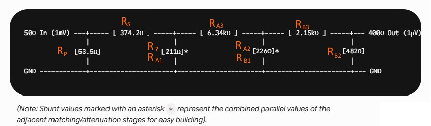
Footnotes:
Page: /Antenna_matching/6/6.shtml
Last modified: Sunday, 5 Jul 2026