

This page documents MY install of the selectivity switch. I had a really hard time making the hardware, the schematic and my thinking connect with each other.
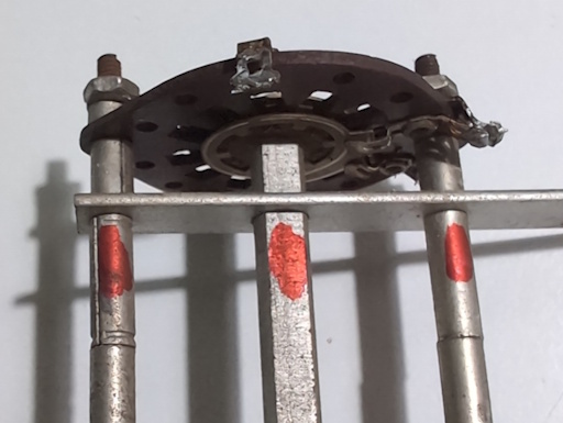
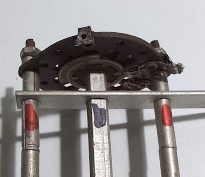
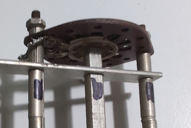
Switch has 3 wafers (front (of radio), middle and rear) with each having 2 sides (front, back)
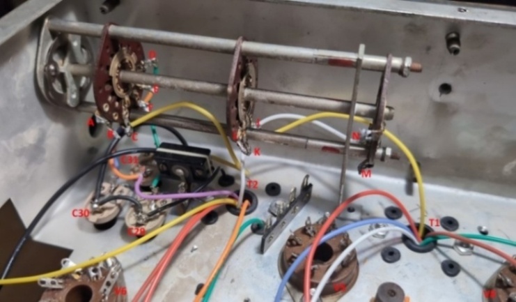
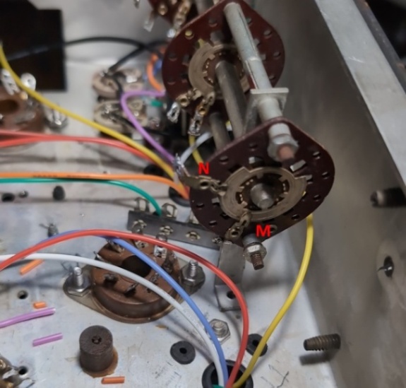
The letters used in the photos to identify switch terminals are of my own invention and match the notes on the schematic included on this page (I hope)
First wafer, closest to front of radio:
Middle wafer:


Rear wafer:


Schematic mark up:

Switch is mounted close to chassis wall so I use "chassis side" and "open side.". It's not possible to solder the chassis side once switch is installed.
It appears that SW9-2 is the middle wafer and since terminal K connects to the center rotor ring on each side, there's actually only one switch
It appears that SW9-3 is the front wafer and the center rotor rings are connected via pin C but the schematic shows two switches.
If so, the rear wafer is SW9-1
If the rotor is in a position such that pin K is connected to J (middle wafer, front) then the switch is in position #1 or 'I.F. Broad'. On my switch, while in position #1, I have black marker on one side of the frame and shaft and red marker on the opposite side. If the colors line up, it's in position #1. I realize this is ridiculous overkill but I REALLY REALLY don't want to redo this when I'm trying to calibrate the radio.
Initial intent is:
AFT = After switch is installed.
BEF = Before switch is installed.
1ST = Solder with switch hanging loose and in position.
WHT_S = white stranded
RED_S= red stranded
YEL_S = yellow stranded
BRN_S = brown stranded
BLU_S = blue stranded
GRN_S = green stranded
BLK_S = black stranded, BLK = black solid
ORG_S = orange stranded
Pins G-I, O not used
Pin A: AFT WHT_S from T2
Pin B: AFT ??? goes to R20 & V6 pin 4.
Pin C: BEF BLK_S goes to junction of C31 & CX1.
Pin D: BEF GRN_S goes to C29
Pin E: BEF ??? goes to a terminal with C107, C31 and purple wire from T2
Pin F: BEF BLU_S goes to C30
Pin J: 1ST YEL_S from T2
Pin K: BEF ??? goes to C106 (inside T2?) & R18 & C28. (Middle wafer, inner ring)Pin L: AFT BRN_S from T2.
Pin M: AFT ??? goes to R15 & C25. (Rear wafer, inner ring)
Pin N: AFTBRN_S from T1.
Pin P: AFTWHT_S from T1.
Pin A: gets the white wire from T2
B goes to R20 & V6 pin 4 & the crystal. The black wire from the front panel control C31 connects as well.
L gets the brown wire from T2
K gets the red wire from T2
N gets the brown wire from T1
P gets the white wire from T1
M goes to junction of C25 & R15
Mickey Lane, 28 Sep 2025, Zephyrhills, FL
Page: /Selectivity_switch/Selectivity_switch.shtml
Last modified: Friday, 24 Apr 2026